+86-15134803151
- Chinese
- French
- German
- Portuguese
- Spanish
- Russian
- Japanese
- Korean
- Arabic
- Irish
- Greek
- Turkish
- Italian
- Danish
- Romanian
- Indonesian
- Czech
- Afrikaans
- Swedish
- Polish
- Basque
- Catalan
- Esperanto
- Hindi
- Lao
- Albanian
- Amharic
- Armenian
- Azerbaijani
- Belarusian
- Bengali
- Bosnian
- Bulgarian
- Cebuano
- Chichewa
- Corsican
- Croatian
- Dutch
- Estonian
- Filipino
- Finnish
- Frisian
- Galician
- Georgian
- Gujarati
- Haitian
- Hausa
- Hawaiian
- Hebrew
- Hmong
- Hungarian
- Icelandic
- Igbo
- Javanese
- Kannada
- Kazakh
- Khmer
- Kurdish
- Kyrgyz
- Latin
- Latvian
- Lithuanian
- Luxembou..
- Macedonian
- Malagasy
- Malay
- Malayalam
- Maltese
- Maori
- Marathi
- Mongolian
- Burmese
- Nepali
- Norwegian
- Pashto
- Persian
- Punjabi
- Serbian
- Sesotho
- Sinhala
- Slovak
- Slovenian
- Somali
- Samoan
- Scots Gaelic
- Shona
- Sindhi
- Sundanese
- Swahili
- Tajik
- Tamil
- Telugu
- Thai
- Ukrainian
- Urdu
- Uzbek
- Vietnamese
- Welsh
- Xhosa
- Yiddish
- Yoruba
- Zulu
- Kinyarwanda
- Tatar
- Oriya
- Turkmen
- Uyghur


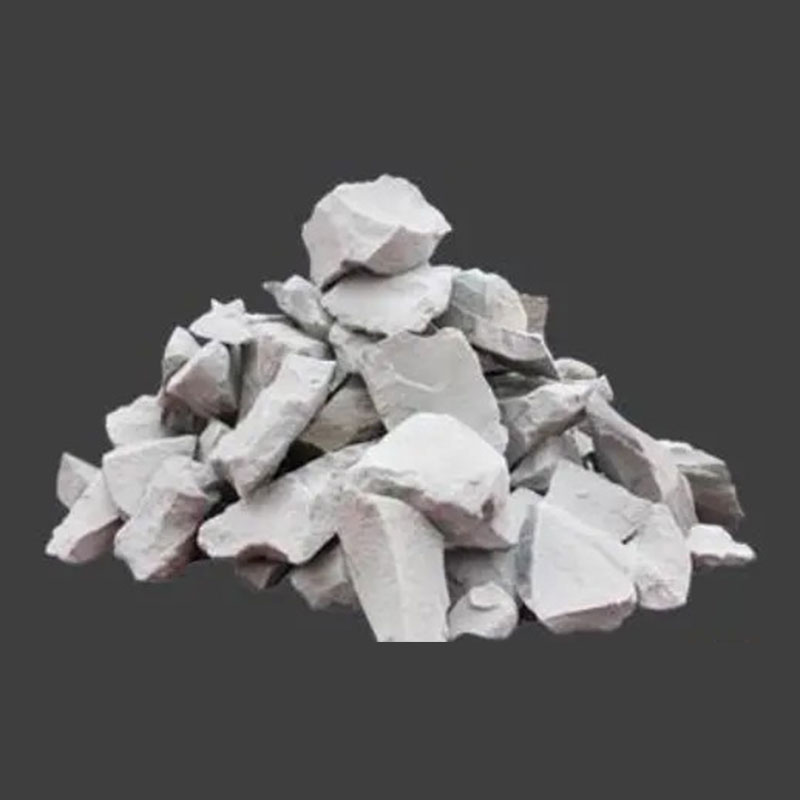
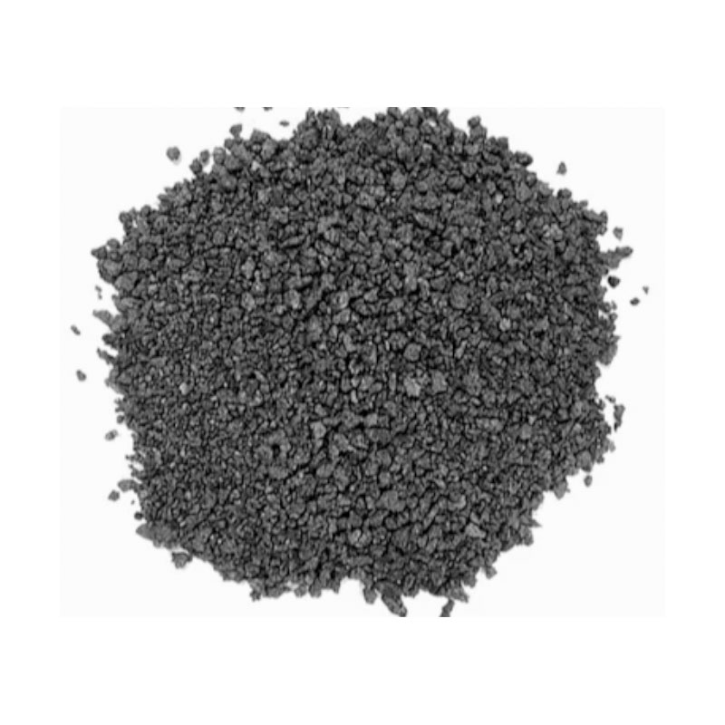
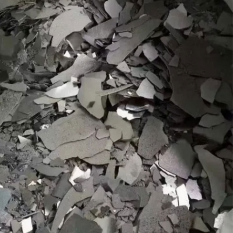
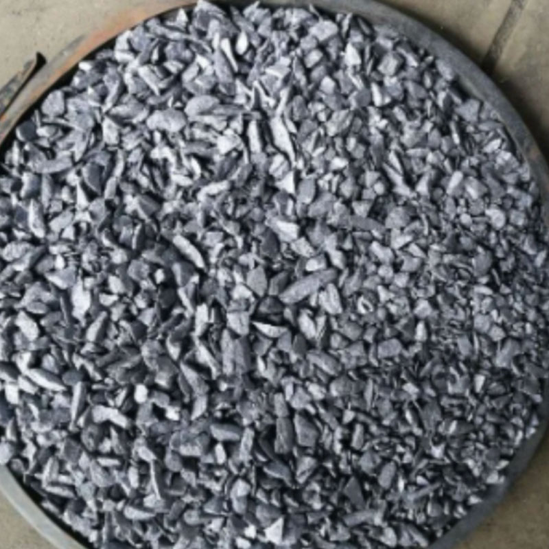
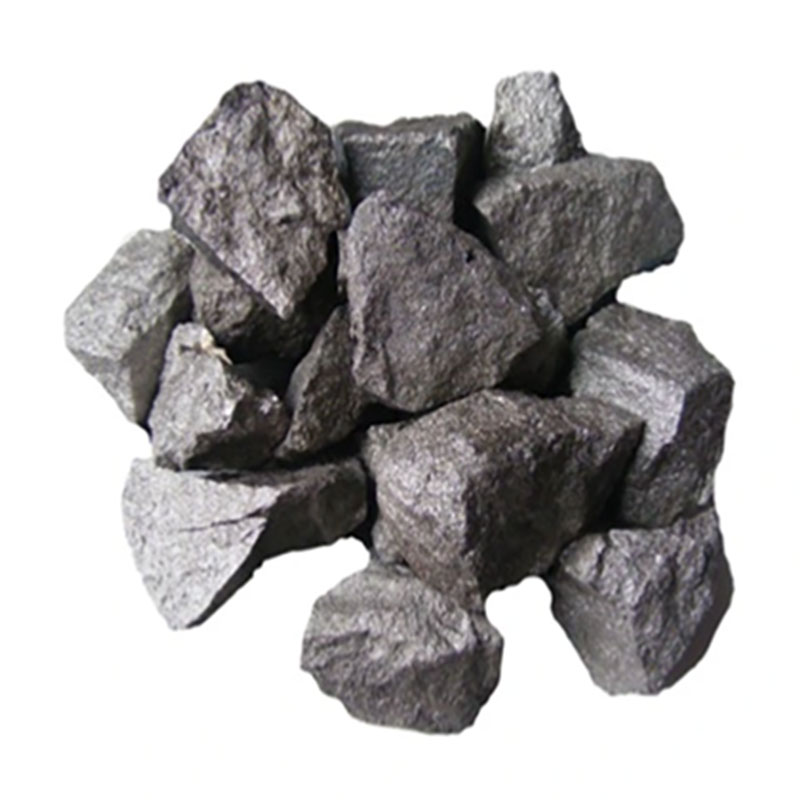
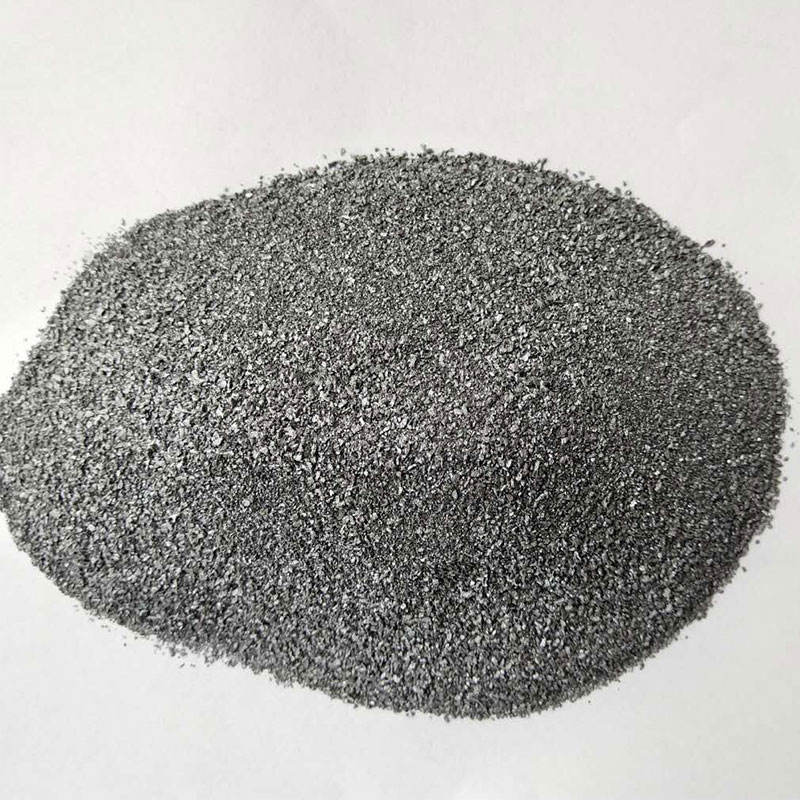
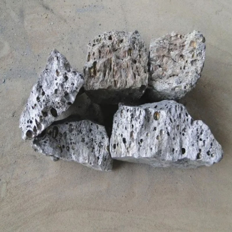
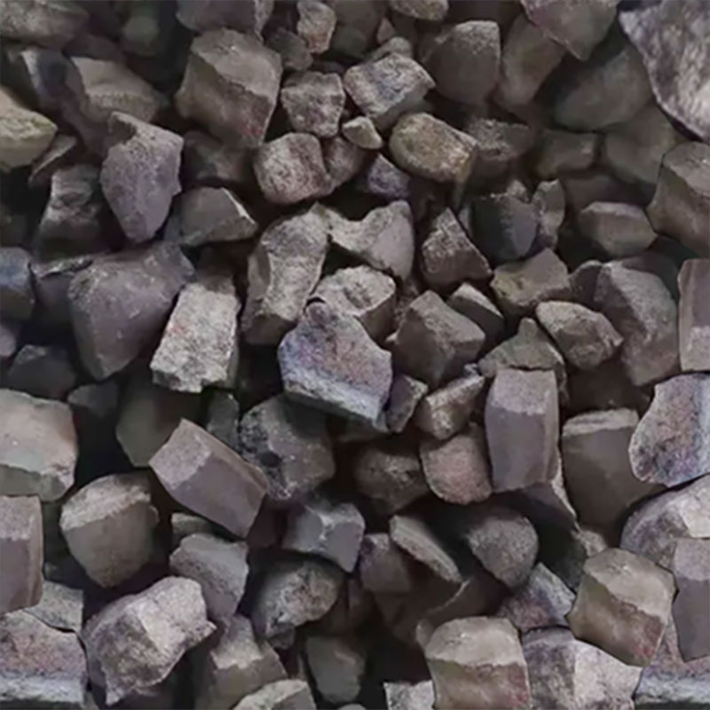
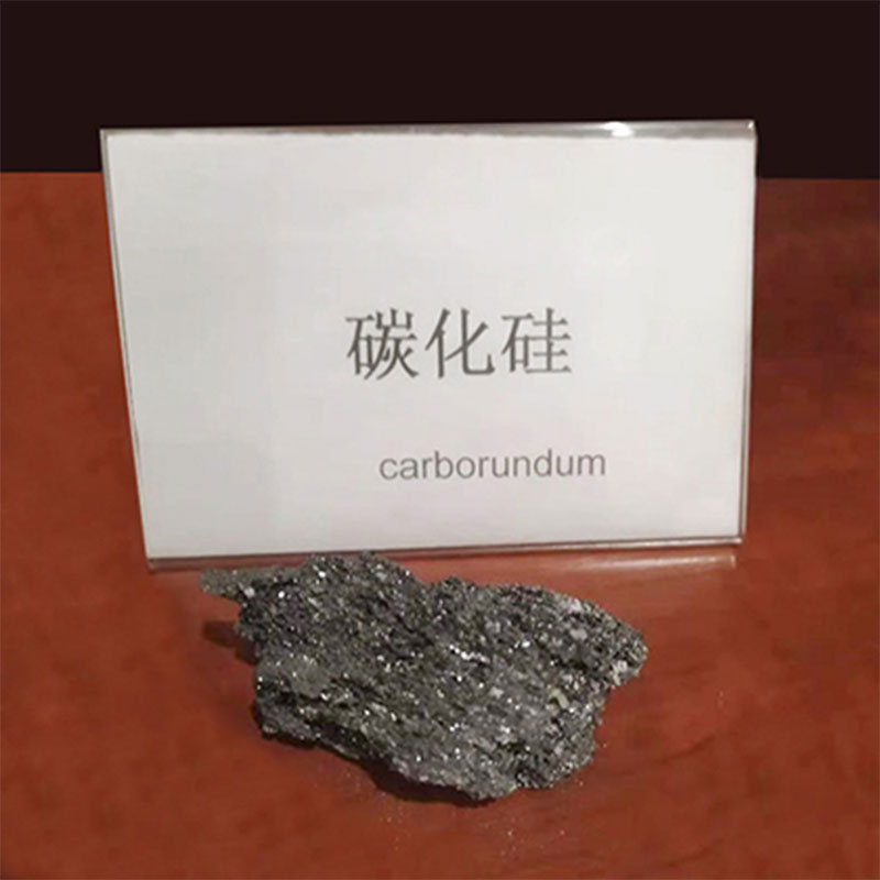
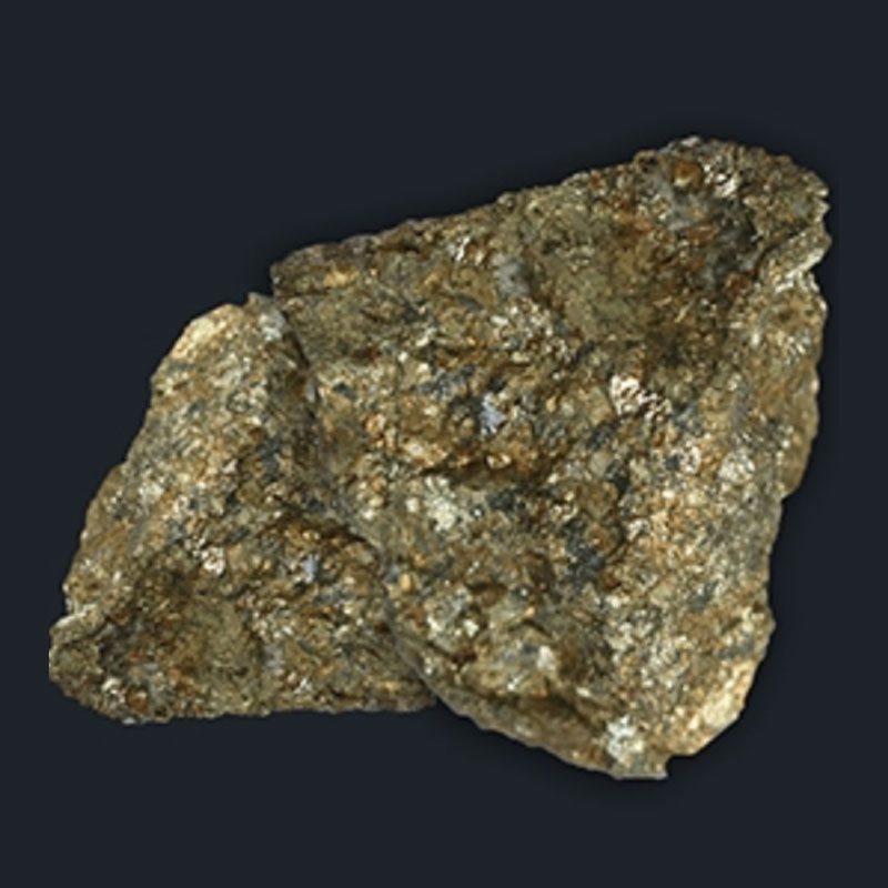
fe silicon
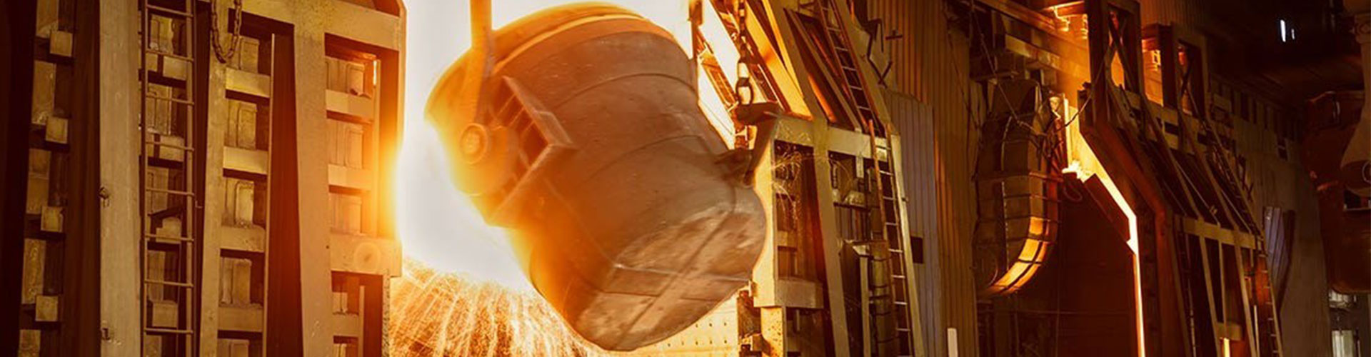
Understanding and Utilizing FE Silicon
This comprehensive guide explores the world of front-end (FE) silicon, covering its properties, applications, and future implications. We delve into the manufacturing processes, key performance indicators, and compare different types of FE silicon, providing insights for professionals and enthusiasts alike. Learn about the advancements driving innovation in this crucial semiconductor technology.
What is Front-End (FE) Silicon?
FE silicon refers to the initial stages of silicon wafer manufacturing. It encompasses processes like crystal growth, wafer slicing, lapping, polishing, and etching. These steps are crucial for creating the high-quality, defect-free silicon substrates necessary for integrated circuits (ICs). The quality of the FE silicon directly impacts the performance and reliability of the final electronic devices. Variations in purity, crystal structure, and surface finish significantly influence device characteristics.
Key Properties and Characteristics of FE Silicon
Several key properties dictate the suitability of FE silicon for various applications:
- Crystal Orientation: The orientation of the silicon crystal lattice affects the electrical and mechanical properties of the final device. Common orientations include (100) and (111).
- Resistivity: The resistivity of the silicon determines its ability to conduct electricity. This is crucial in determining the doping levels required during the backend processes.
- Surface Quality: A smooth, defect-free surface is essential for optimal device performance. Surface roughness and defects can lead to reduced yields and unreliable devices.
- Thickness and Diameter: The thickness and diameter of the silicon wafers are standardized to facilitate efficient manufacturing processes. Common sizes include 200mm, 300mm, and even larger.
Applications of FE Silicon
High-quality FE silicon is the foundation for a vast array of electronic devices:
- Microprocessors: The brains of computers and smartphones rely on incredibly sophisticated FE silicon substrates.
- Memory Chips: From RAM to flash storage, the performance and capacity of memory devices are intrinsically linked to the quality of the FE silicon used.
- Sensors: Various sensors, from those found in automobiles to those used in medical devices, leverage the properties of carefully processed FE silicon.
- Power Electronics: Power management ICs and other components require high-quality FE silicon capable of withstanding high currents and voltages.
Comparison of Different FE Silicon Types
Different manufacturing processes and specifications result in varying grades of FE silicon. These differences impact cost and performance.
| Property | Type A | Type B |
|---|---|---|
| Resistivity (Ω·cm) | 1-10 | 10-100 |
| Surface Roughness (nm) | <0.5 | <1.0 |
| Defect Density (cm?2) | <100 | <500 |
Note: This is a simplified comparison. Actual specifications vary significantly based on manufacturer and application requirements.
The Future of FE Silicon
Ongoing research and development continuously improve the quality and capabilities of FE silicon. Advancements in crystal growth techniques, surface treatment methods, and defect control promise even higher performance and lower costs. Explore the possibilities of Inner Mongolia Xinxin Silicon Industry Co.,Ltd for high-quality FE silicon solutions.
The transition to larger diameter wafers, improved purity levels, and novel manufacturing techniques are driving the future of FE silicon and its applications in advanced electronics.
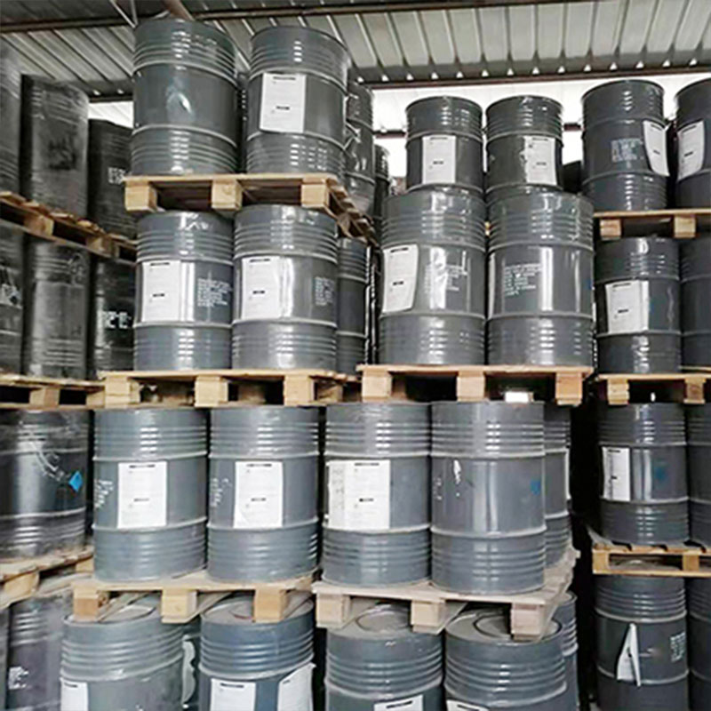
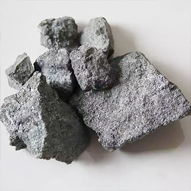
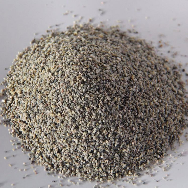
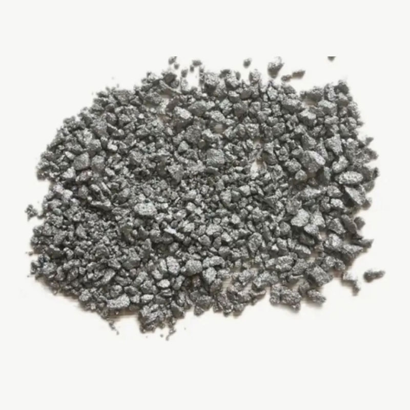
Related products
Related products